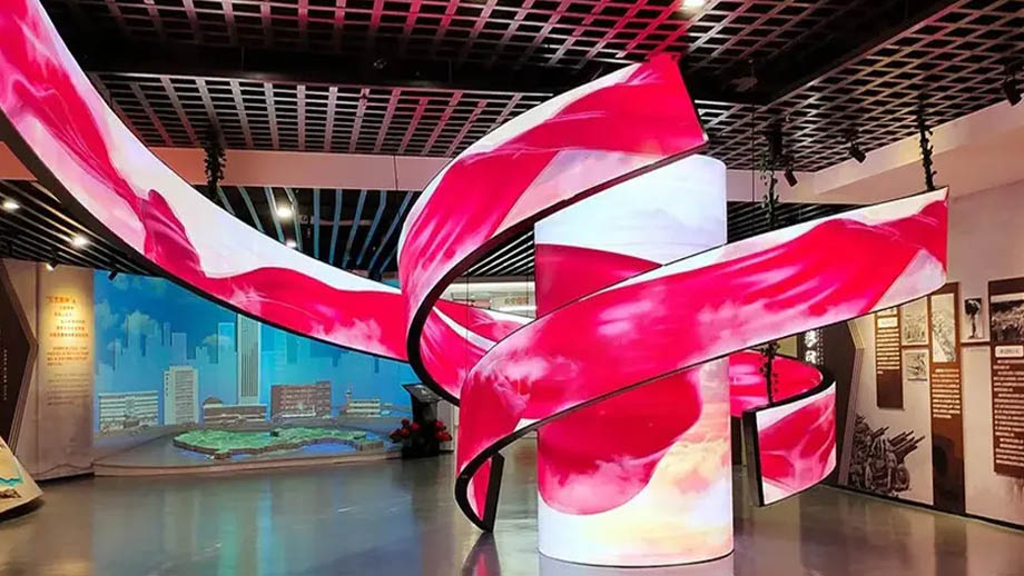



The performance of an LED display cannot be separated from its LED packaging technology.
By choosing an appropriate LED packaging technology, the brightness, color performance and energy consumption of the LED screen can be greatly improved.
Today we together through this article to understand, LED packaging technology in the end what.
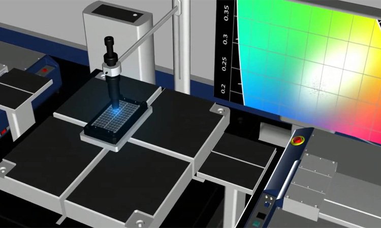
The concept of LED packaging technology
LED packaging technology refers to a series of operations in the production stage, the LED chip, electrodes and optical components such as components encapsulated in protective packaging materials, the composition of the complete LED device, but also has the electrical connection, heat dissipation and optical function.
With LED packaging technology, the optical conversion rate of the LED bead will be higher and the device will be more stable and reliable.
LED packaging technology core steps
Chip Binding
Wafer Cleaning and Inspection
Before we start the LED packaging technology, we need to inspect all the LED chips to make sure that they conform to the dimensions on the drawings, electrode sizes, and to make sure that the electrode patterns of the LED chips are intact and missing.
After screening out the LED chips that meet the process requirements, then clean them so that there is no any oil or dust on its surface.
Wafer Positioning and Bonding
After doing the cleaning work, use the wafer fixing machine to accurately place the LED chip in the originally designed position, apply a layer of conductive adhesive, and fix the LED chip on the substrate.
This process of LED chips placed in the position of high precision requirements, so you need to use high precision wafer fixing machine, once the position and angle of the LED chip placed deviation, will lead to the subsequent LED display light-emitting effect and light-emitting efficiency is affected.
Metal Wire Soldering
Metal Wire Selection and Soldering Process
We usually choose a slower oxidizing and higher purity metal wire as the connecting wire to connect the electrodes on the surface of the LED with the bracket.
This kind of connecting wire we will use copper, silver, gold and other more stable metal, of which, copper wire is the most cost-effective, the widest range of applications, the stability of the gold wire is the best, but the price is expensive, and therefore less used.
Welding process generally use thermal ultrasonic bonding technology, this technology is the use of heat, pressure, and ultrasonic waves, the metal wire and LED chips and brackets welded together.
Welding quality inspection
After welding is completed, the welding point should be inspected to ensure that there is no leakage of welding, if there is leakage of welding, then make up the welding, or there is leakage of tin, weld slag and other poor appearance of the situation also needs to be repaired accordingly.
Encapsulation Molding
Mold Design and Manufacturing
According to the design requirements of the LED device to design a reasonable mold, and then the mold will be made.
Injection/filling of encapsulation materials
LED encapsulation materials have a great impact on the performance and service life of LED modules, and the most common encapsulation materials are plastic, metal and glass.
Plastic encapsulation is the most common encapsulation material, it is cheap, good light transmittance, for all kinds of occasions are applicable; metal encapsulation usually use aluminum, copper and other metals, heat dissipation is good, will not let the LED chip overheating damage; glass encapsulation light transmittance is high, stability is good, but the production cost is more expensive.
After selecting the appropriate encapsulation material, through injection molding or filling of the encapsulation material to cover the LED chip to form a complete encapsulation structure.
Post-encapsulation Processing
The encapsulated LED device needs to undergo strict quality testing to ensure that it functions properly, and then undergo aging testing to reinforce the stability and service life of the LED.
Optical Processing
Lens Design and Manufacturing
Designing a suitable lens mounting that meets the characteristics of the LED can increase the light aggregation and improve the utilization of light.
Optical Film Coating
LED devices manufactured by LED packaging technology can increase brightness and reduce color temperature by coating one or more layers of optical film layers on the surface.
Optical Performance Testing
Before leaving the factory, LED devices also need to use special optical performance testing instruments to check whether the parameters of brightness, color temperature and screen uniformity meet the design requirements.
Features of LED packaging technology
High accuracy
The fixed position of LED lamp beads affects the resolution and uniformity of the subsequent LED screen, which are closely related to the display effect, using LED packaging technology can ensure that each LED lamp bead is accurately fixed in the corresponding position, to ensure that the brightness, color uniformity and beauty of the LED screen.
High reliability
After LED packaging technology, LED screen can prevent the environmental moisture, dust and other foreign substances invasion, resulting in corrosion of electronic devices; in addition, LED packaging technology can also maintain a certain temperature stability, enhance the operational reliability of the LED display.
Energy saving and environmental protection
LED packaging technology can increase the utilization rate of light energy of LED lamp beads, increase the utilization rate of energy conversion, thereby reducing energy consumption, more energy-saving and environmentally friendly.
Versatility
development to today, LED packaging technology has a variety of technology types, according to the characteristics of the use of the LED screen to choose the LED packaging technology, in addition, if there are special requirements, you can also contact JYLED customized LED packaging technology suitable for special scenarios.

Types of LED packaging technology
DIP package (dual-row in-line package)
DIP package is a relatively early LED packaging technology, you need to manually insert the LED lamp beads fixed to the PCB board, its advantages are simple process, low cost, high brightness, good protection performance, not easy to be damaged, but it is not easy to watch the angle of view Fixed accurate, only suitable for outdoor large-pitch LED display.

SMD package (surface mount device)
SMD package is one of the most common LED packaging technology on the market, which first encapsulates the LED chip into a lamp bead, and then welds the LED lamp bead to the substrate on a large scale through the SMD machine.
SMD packaging technology has been developed for a long time, the process is more mature, and the scale operation reduces the manufacturing cost.
The LED screen using SMD encapsulation technology has good heat dissipation, and the LED light beads display rich and vivid colors independently, which is used in a variety of scenarios, but the SMD encapsulation technology can not complete the pixel pitch of 1mm below the small-pitch LED display production.

GOB encapsulation (board sticking)
GOB encapsulation technology refers to the LED chip mounted on the module after a whole module using a special conductive adhesive cover sealing, forming an effective protection, and then the surface for frosted treatment, after the second surface of the optical treatment of the LED module will be better light transmission.
The use of GOB encapsulation technology LED display surface smooth without obvious particles, but also can effectively waterproof, dustproof, anti-impact.
However, due to its low integration, it is only suitable for medium power LED screen.

COB packaging (chip-on-board)
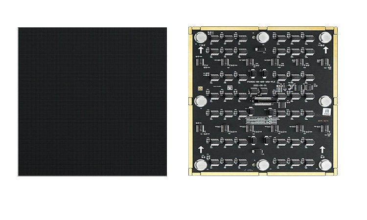
COB packaging refers to multiple LED chips directly bonded to the substrate to form a single LED block, this LED packaging technology can save a lot of space, can be packaged below 1mm small pitch LED display, it can also enhance the optical output, after the COB packaging technology LED display screen picture is clearer and softer! COB packaging technology, but the encapsulated individual LED block only a single circuit, so it is not conducive to the diversity of LED bead color.
COB package currently accounts for about 45% of the market, because COB package technology is more mature, and low cost, high quality, more popular in the market.
Flip-chip COB package (Flip COB)
Flip-chip COB package refers to the LED chip directly pressed together on the substrate, this packaging technology does not require lead bonding, but also discard the past use of conductive adhesive lamination.
It has the advantages of small size, high performance, strong stability, to meet the characteristics of high-power LED use, but Flip-chip COB packaging technology than COB packaging technology, Flip-chip COB packaging technology manufacturing process is more complex.
WLP packaging (wafer level packaging)
WLP packaging refers to packaging and testing directly on the wafer, and then cut into individual components, this LED packaging technology can save a certain amount of process and cost, and a large number of reduced LED size, the development of this technology for small-pitch LED display is a qualitative leap in technology.
COF packaging (flexible chip)
COF packaging refers to a number of medium-power LED chips centrally encapsulated in a flexible circuit board, flexible base plate means more possibilities for LED screen modeling, which can adapt to a variety of strange shapes and installation environments, and COF packaging technology LED screen is usually characterized by high thermal conductivity, high luminous efficacy, and uniformity of light, and so on.
The development trend of LED packaging technology
miniaturization
Even if the picture of LED display screen is now high definition enough, more clear and detailed picture quality is still always the goal pursued by the market, which also means that the LED module needs smaller pixel pitch and higher pixel density, and the realization of these needs LED packaging technology The LED packaging technology needs to be more miniaturized to achieve this.
And the higher the integration of LED beads, the lower the energy consumption, LED display more energy efficient and environmentally friendly.
Intelligent
Intelligence is now the development trend of all electronic devices, the rapid rise of artificial intelligence technology, so that electronic devices become more intelligent and convenient.
LED display also need to follow the pace of the times, the future of LED packaging technology will have more features, such as remote control, automatically follow the environment to adjust the display brightness and so on.
Green
LED packaging technology in the past used basically non-polluting, harmless to the human body of environmentally friendly materials, in addition to the future should be added to the material recycling routes, recyclable resources will be repeatedly utilized to avoid material waste.
Both reduce the manufacturing cost, but also reduce the waste of resources, so that the LED display in energy saving and environmental protection have greater progress.
Customization
People’s demand for personalization is increasing, LED packaging technology also need to gradually towards the direction of customization, for different user needs to develop different LED packaging technology solutions to meet the different scenes of customers, different needs LED display applications.

Conclusion
LED packaging technology is a tedious process, which is closely related to the performance of the final LED display.
There is no absolute good or bad LED packaging technology, the choice of them is more for the consideration of cost and applicability. If after reading this article you still have questions, you can consult the professional and technical personnel of JYLED.